How to create better PCB designs
Motivation
I have my first request for a copy of AnywhereAmps Alpha. I wouldn’t want to spend another 10h in building it, so I decided to invest the time into speeding up the manufacturing process. I figured out I could save about an hour per amp if I had the circuit board produced for me. Unfortunately, switching the Circuit Board from hand cutting, milling, drilling, soldering to a PCB design cost me twice as much time compared to a full build already. And I don’t even know if this works yet. But let’s start at the beginning.
Requirements on the new PCB
The PCB shall contain
- the preamp circuit as designed for AnywhereAmps Alpha
- the two-way crossover circuits as designed for future AnywhereAmps Beta
- a switching buck converter to provide 9V DC for the aux effects
- a Power supervisory circuit protecting both battery and PCB from overload, short circuit, under voltage, reverse voltage
This way, I want to gradually professionalize the electronics. I intend to use the same PCB for any variant of AnywhereAmps. In addition, I would get rid of some external components that I had to manufacture and place by hand: Fuse, high-current capable power switch, the 9V regulator and its cooling, and some wiring.
Component selection
Buck Converter
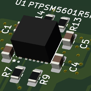
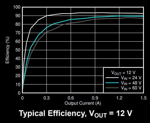 I searched the web for a low-EMI (ElectroMagnetic Interference) switching buck converter with an output of >1A @9V. A linear regulator would have been less noisy, but at a nominal battery voltage of 18V I would have to cope with >9W of thermal losses worst case. Plus, this solution wouldn’t have been battery-saving at all. I selected a (costy) design that has all necessary components in-a-box so I just had to get the PCB layout right for EMI reduction. Add a couple of bypass capacitors and a resistor divider for the target voltage setpoint. Done! (I thought at that time. Here’s how it actually turned out)
Power Supervisor
 The only protection for my amps was a fuse until now, its value set to the highest “normal” current I expected in the circuits. In the early prototype phases I killed some opamps by accidentally applying a reverse voltage. And I want to avoid to totally drain the battery pack when I forget to look at the charge indicators. So I selected a power supervisor IC that would detect any undervoltage or fault condition and protect both circuits and battery from damage.
Passive components grouping
I learned that manufacturing a PCB with many different parts would be more expensive and more prone to errors than using less different parts, even if the total number of parts increased this way. So I redesigned many values and re-did the simulation for the audio preamp with these new values. Finally, I was able to break it down from 8/5 to 3 different resistor and 3 different capacitor values!
Capacitors, again
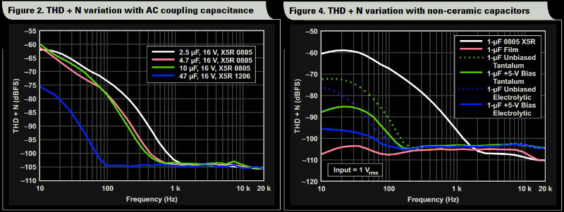
I first used MLCC (Multilayer ceramic capacitors) in my design, both for bypass, and for the audio decoupling capacitors. After again reading the documents I pointed out in my preamp design considerations post, I realized that this capacitor design seems to have trouble with distortion on audio signals. The image below shows a comparison of different capacitor types and sizes. You see that film capacitors have the best performance and MLCCs are worst. As I wasn’t able to find film capacitors with the size I needed on a SMD footprint, and aluminium electrolytic caps were too large, I selected polarized tantalum capacitors. For the bypass uses I selected low-ESR types.
Circuit design
I chose the open-source software KiCad as an Electronic Design Automation tool and redrew all my existing circuit plans, adding the components described above. Look how the amplifier section only fills the right half of the schematics while the left half is devoted to power supply and supervisory circuits.
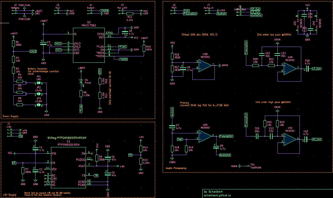
I tried to get the schematics as neat as possible to make them easy to read. I used global labels a lot and added connectors for simplified mounting.
PCB design
This was the hardest part for me. I never designed a PCB for audio usage before, so I had to read a lot of guidelines before I started.
How tos and tutorials
I list some of them below for your reference:
- noise on PCBs and how to avoid
- how to best place bypass capacitors
- ground plane or not?
- how to handle different grounds for signals, power, etc.
- how to optimize parts placement for soldering
- avoid these pitfalls when designing PCBs
- how much current can my track handle with this width?
- some PCB design specifications for manufacturability
- PCB manufacturing is getting harder with smaller structures
I tried to apply those design guidelines the best I could.
AnywhereAmps PCB explained
The result after a couple of evenings:
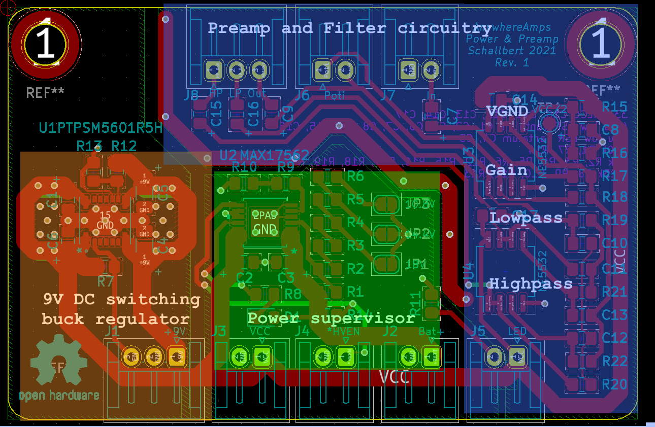
I separated the PCB into three zones.
- Left: the 9V switching regulator, following its reference design (datasheet) it would create a current circle around itself using the bypass capacitors and cancel out most of the EMI. Look at the thermal design, it has a lot of copper and quite some vias to get the heat conducted away from the die.
- Center: The power terminals and supervisory circuit. I placed solder jumpers to select the nominal battery voltage for the undervoltage detection.
- Right and top: Preamp and analog signal circuitry, separated by the other electronics stuff using a thick ground track on the top copper and an own ground plane on the bottom. I hope this is enough…
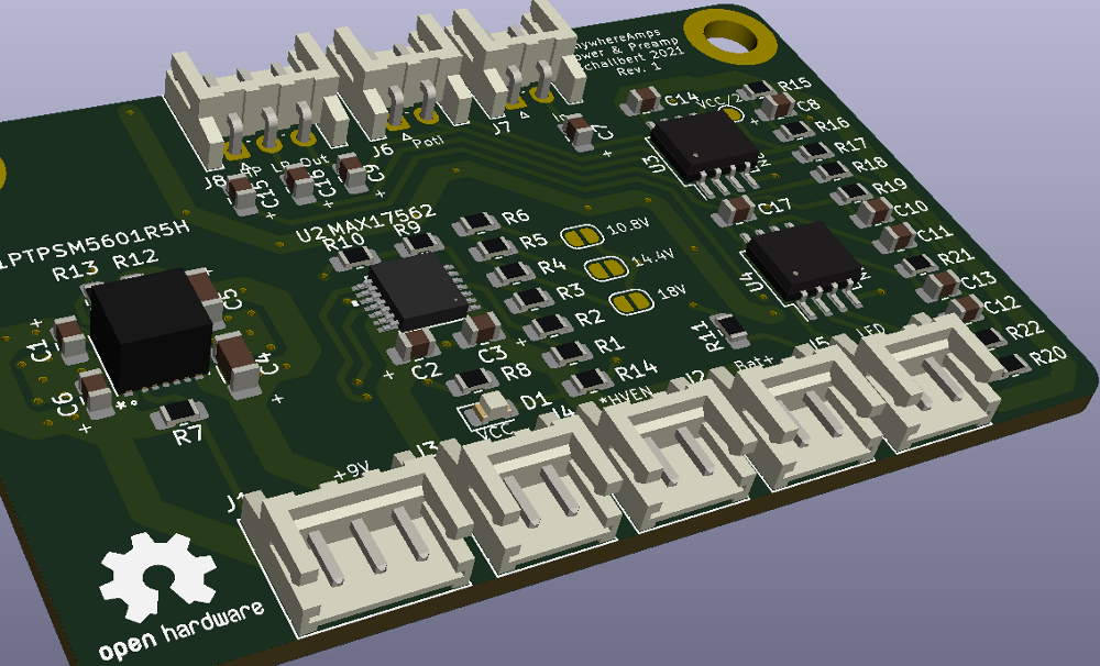
As I’ll hand-solder the first prototypes to check if it all works OK, I used “big” 0805 SMD components. I increased the space in between them by more than the PCB specification would demand. Unfortunately, the highly integrated power ICs were not available in “hobby soldering electronics” sizes so I’ll have to go through some pain there :(
So this is how it will look like. The PCB size will be 45mm x 69mm.
Contribute or download
All the CAD models and schematics are open source and available for download and your contributions on my dedicated Github repository.
Up next: PCB delivered and soldered